Michael E. Byczek
Attorney at Law
The following are recent U.S. patents that involve quantum computers. The full patent was downloaded from www.uspto.gov and is available to view on this page. Each patent is summarized with the official abstract and one representative drawing (click to view full-size). Also included are pending patents, identified as "publication". Michael E. Byczek was not involved with any of these patents. This information is being used to explain Quantum Computers through representative patents that have been filed with the U.S. Patent and Trademark Office (USPTO).
Intel
Apparatus and Method for Specifying Quantum Operation Parallelism for a Quantum Control Processor
9/5/2023 (US 11,748,649) [30 Claims, 33 Drawing Sheets)]
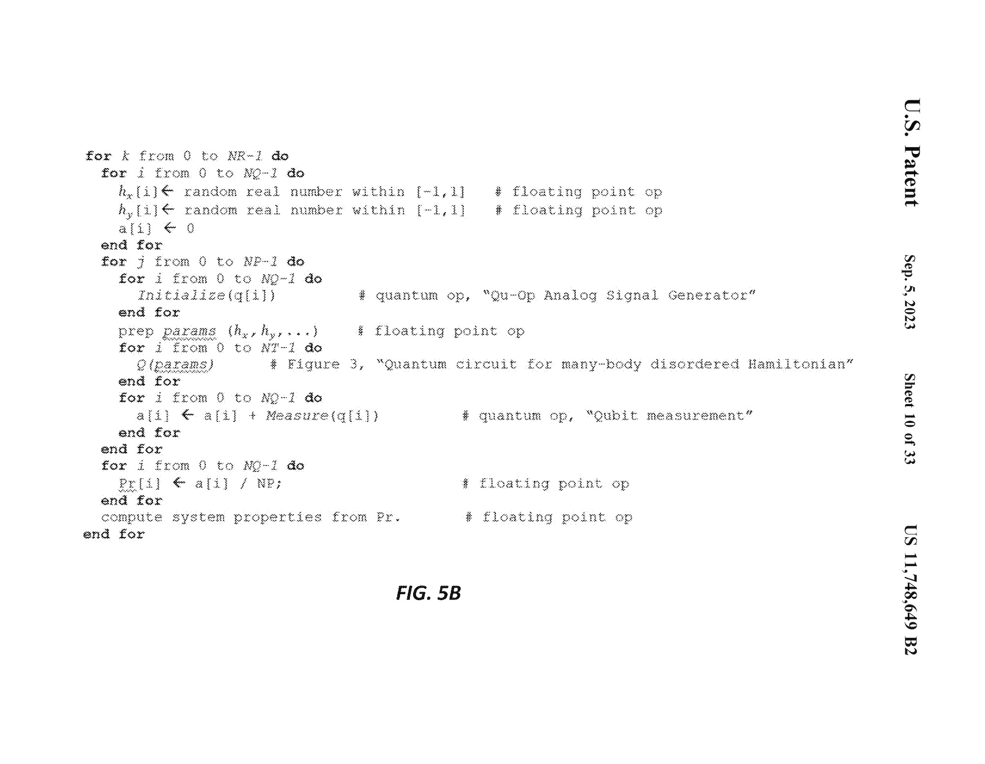
Figure Description: program code to implement the quantum circuit
Abstract: Instruction fetch circuitry to fetch a plurality of quantum instructions from a memory or a cache; slice-based instruction processing circuitry to identify quantum circuit slices comprising sets of one or more of the plurality of quantum instructions; and one or more instruction decoders to decode the quantum instructions to generate quantum microoperations; and quantum execution circuitry to execute sets of the quantum microoperations in parallel based on the quantum circuit slices.
Apparatus and Method for Scalable Qubit Addressing
9/5/2023 (US 11,748,651) [9 Claims, 21 Drawing Sheets]
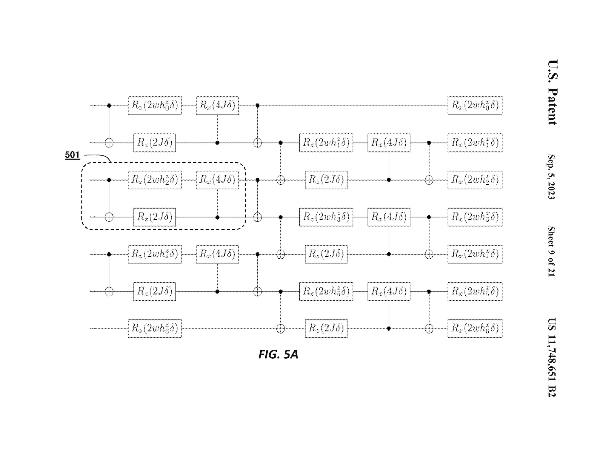
Figure Description: example quantum circuit
Abstract: A decoder comprising quantum instruction decode circuitry to decode quantum instructions to generate quantum micro-operations (uops) and non-quantum decode circuitry to decode non-quantum instructions to generate non-quantum uops; execution circuitry comprising: an address generation unit (AGU) to generate a system memory address responsive to execution of one or more of the non-quantum uops; and quantum index generation circuitry to generate quantum index values responsive to execution of one or more of the quantum ops, each quantum index value uniquely identifying a quantum bit (qubit) in a quantum processor; wherein to generate a first quantum index value for a first quantum uop, the quantum index generation circuitry is to read the first quantum index value from a first architectural register identified by the first quantum uop.
Gate Walls for Quantum Dot Devices
9/5/2023 (US 11,749,721) [25 Claims, 38 Drawing Sheets]
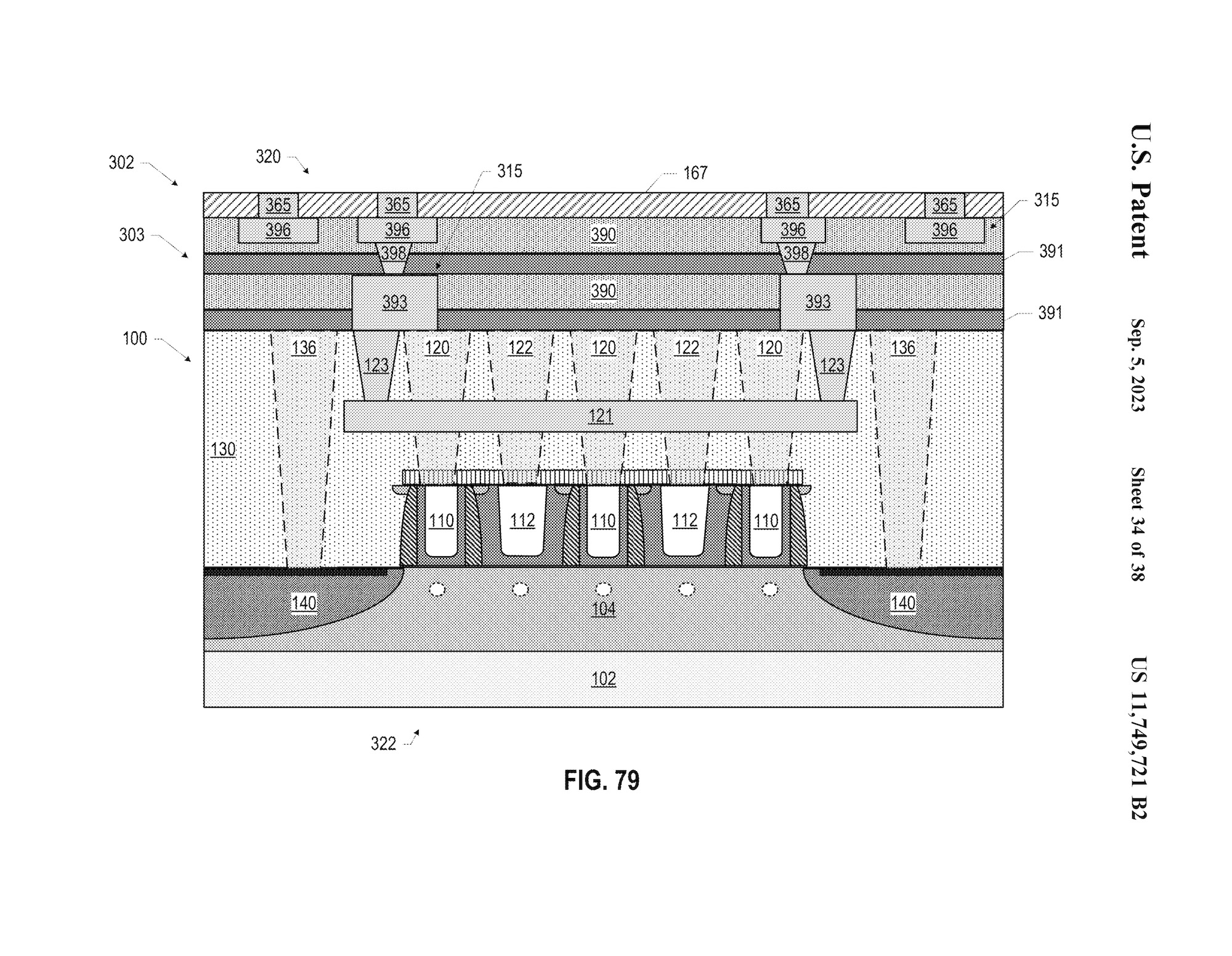
Figure Description: cross-sectional view of a quantum dot device with multiple interconnect layers, in accordance with various embodiments.
Abstract: A quantum dot device may include: a quantum well stack; a first gate and an adjacent second gate above the quantum well stack; and a gate wall between the first gate and the second gate, wherein the gate wall includes a spacer and a capping material, the spacer has a top and a bottom, the bottom of the spacer is between the top of the spacer and the quantum well stack, and the capping material is proximate to the top of the spacer.
Message Index Aware Multi-Hash Accelerator for Post Quantum Cryptography Secure Hash-Based Signing and Verification
9/5/2023 (US 11,750,402) [15 Claims, 15 Drawing Sheets]
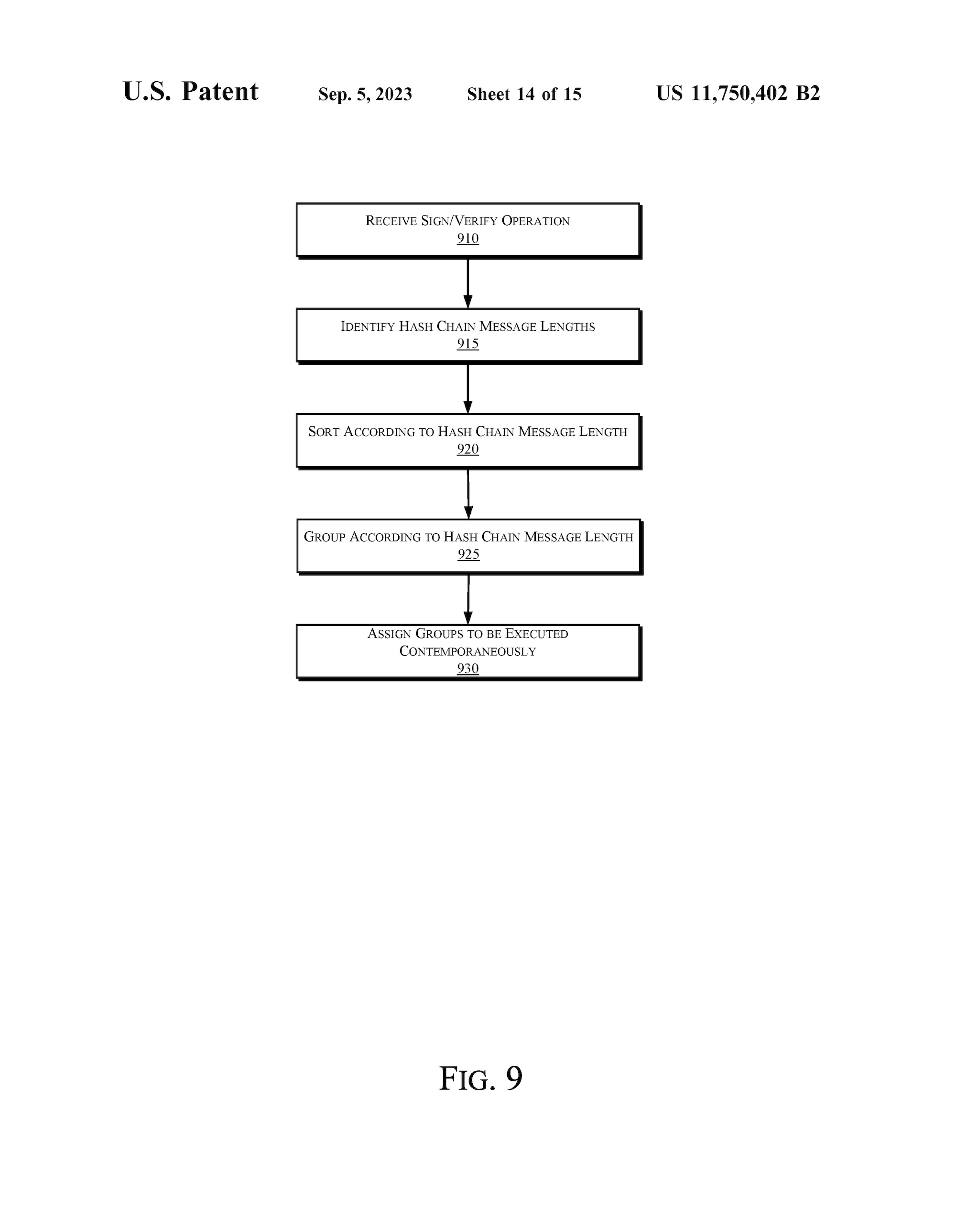
Figure Description: schematic illustration of a flow diagram illustrating operations to implement index-aware hash chain distribution, in accordance with some examples.
Abstract: A computer readable memory, a signature logic to generate a signature to be transmitted in association with a message, the signature logic to apply a hash-based signature scheme to the message using a private key to generate the signature comprising a public key, or a verification logic to verify a signature received in association with the message, the verification logic to apply the hash-based signature scheme to verify the signature using the public key, and an accelerator logic to apply a structured order to at least one set of inputs to the hash-based signature scheme.
Accelerators for Post-Quantum Cryptography Secure Hash-Based Signing and Verification
9/26/2023 (US 11,770,258) [20 Claims, 18 Drawing Sheets]
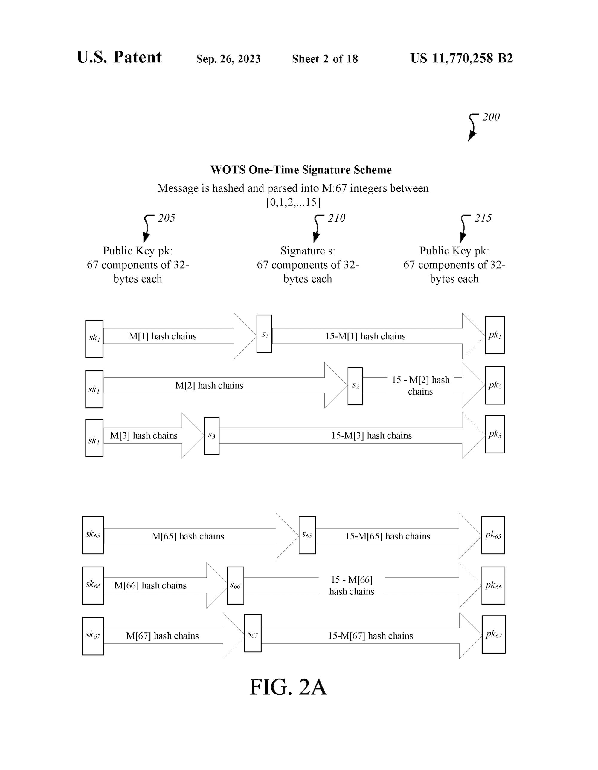
Figure Description: schematic illustration of a one-time signature scheme
Abstract: an apparatus comprises a computer readable memory, hash logic to generate a message hash value based on an input message, signature logic to generate a signature to be transmitted in association with the message, the signature logic to apply a hash-based signature scheme to a private key to generate the signature comprising a public key, and accelerator logic to pre-compute at least one set of inputs to the signature logic.
Quantum Dot Devices
(Publication) - 8/31/2023 (US 2023/0275087)
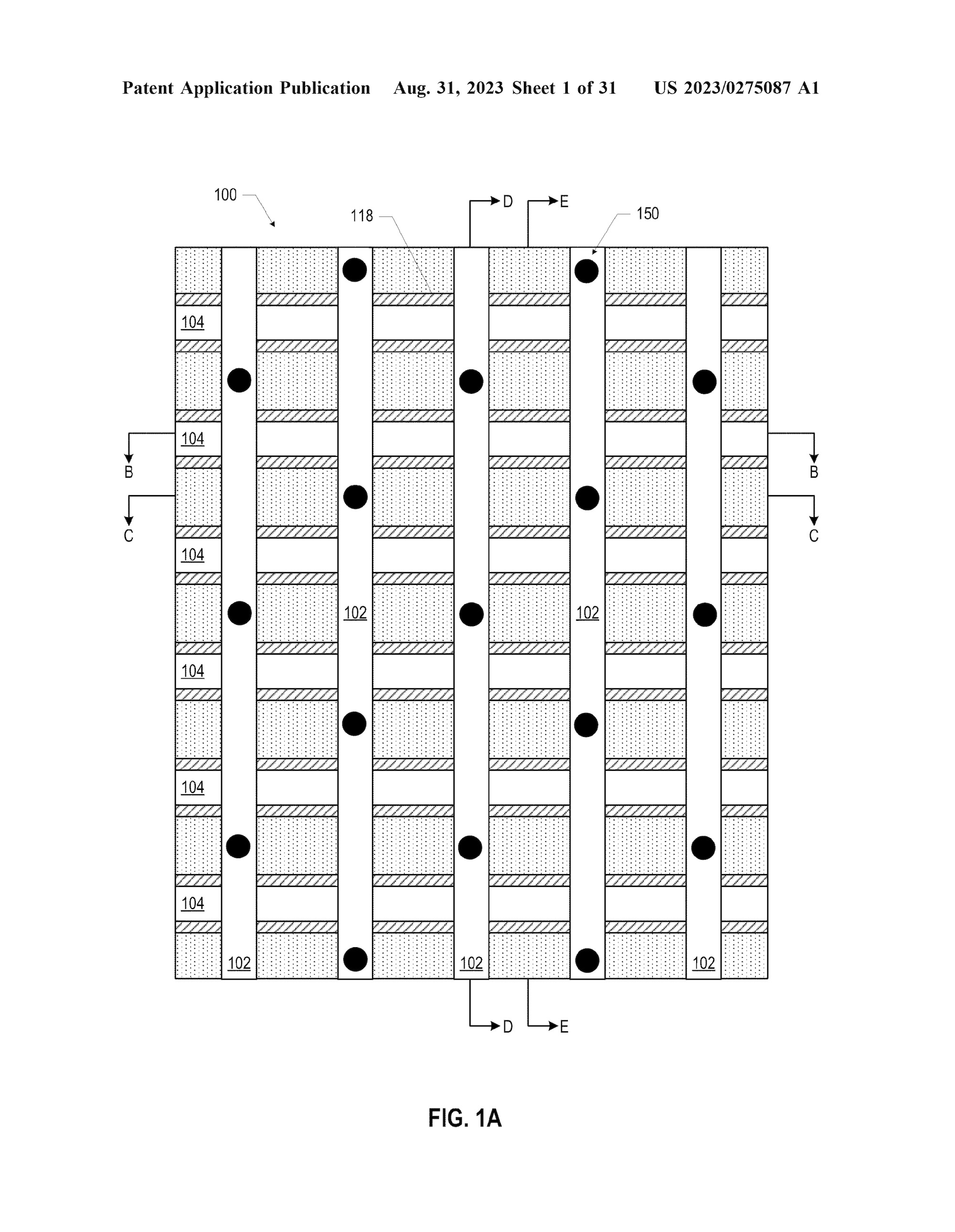
Figure Description: view of a quantum dot device
Abstract: A quantum dot device may include a quantum well stack; a plurality of first gates above the quantum well stack; and a plurality of second gates above the quantum well stack; wherein the plurality of first gates are arranged in electrically continuous rows extending in a first direction, and the plurality of second gates are arranged in electrically continuous rows extending in a second direction perpendicular to the first direction
Quantum Information Processing Device Formation
7/4/2023 (US 11,696,515) [22 Claims, 10 Drawing Sheets]
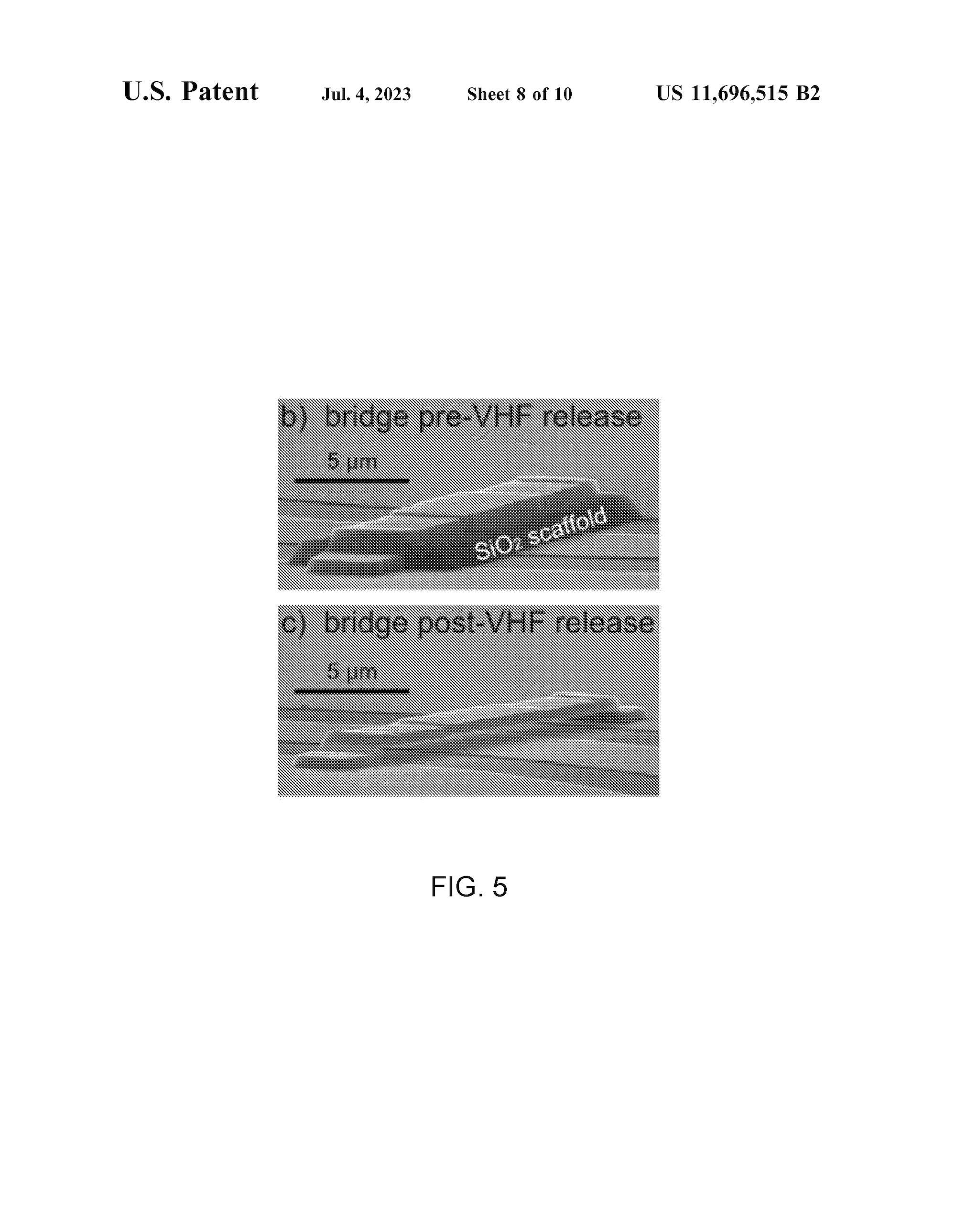
Figure Description: micrograph of an example of a sacrificial silicon dioxide layer supporting an electrically-conductive bridge prior to isotropic VHF etching and subsequent to isotropic VHF etching
Abstract: Providing a first electrically-conductive layer formed of a first electrically-conductive material on a principal surface of a substrate, depositing a layer of dielectric material on the first electrically-conductive material, patterning the layer of dielectric material to form a pad of dielectric material and to reveal a first region of the first electrically-conductive layer, depositing a second electrically-conductive layer on the pad of dielectric material and on the first region of the first electrically-conductive layer, patterning the second electrically-conductive layer and removing the pad of dielectric material using isotropic gas phase etching.
Fabricating a Qubit Coupling Device
9/5/2023 (US 11,751,490) [20 Claims, 6 Drawing Sheets]
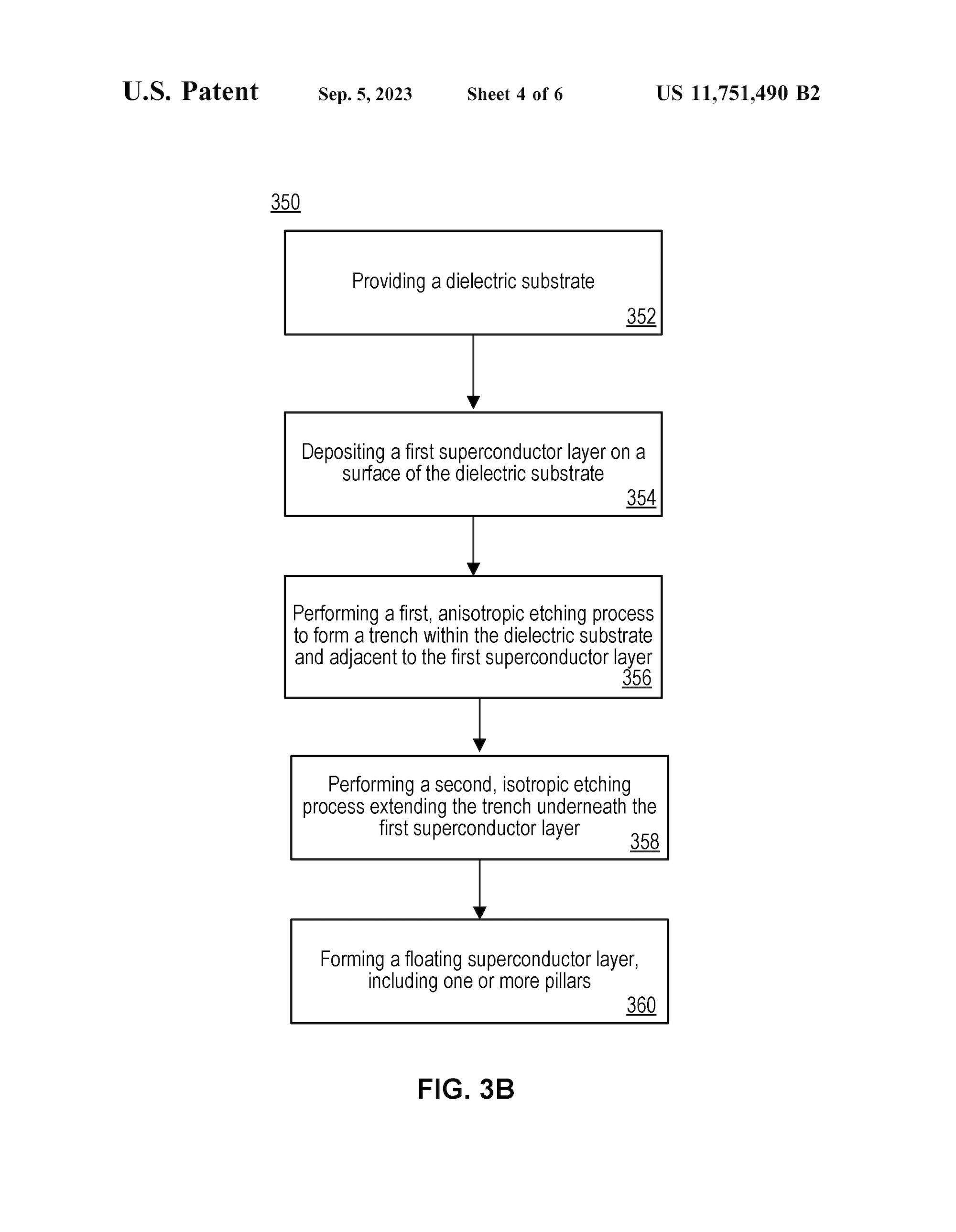
Figure Description: flow diagram of exemplary processes for floating superconductor layers
Abstract: A dielectric substrate including a trench; a first superconductor layer on a surface of the dielectric substrate where an edge of the first super-conductor layer extends along a first direction and at least a portion of the superconductor layer is in contact with the surface of the dielectric substrate, and where the superconductor layer is formed from a superconductor material exhibiting superconductor properties at or below a corresponding critical temperature; a length of the trench within the dielectric substrate is adjacent to and extends along an edge of the first superconductor layer in the first direction, and where the electric permittivity of the trench is less than the electric permittivity o f the dielectric substrate.
Quantum Circuits with Reduced T Gate Count
9/12/2023 (US 11,755,942) [20 Claims, 10 Drawing Sheets]
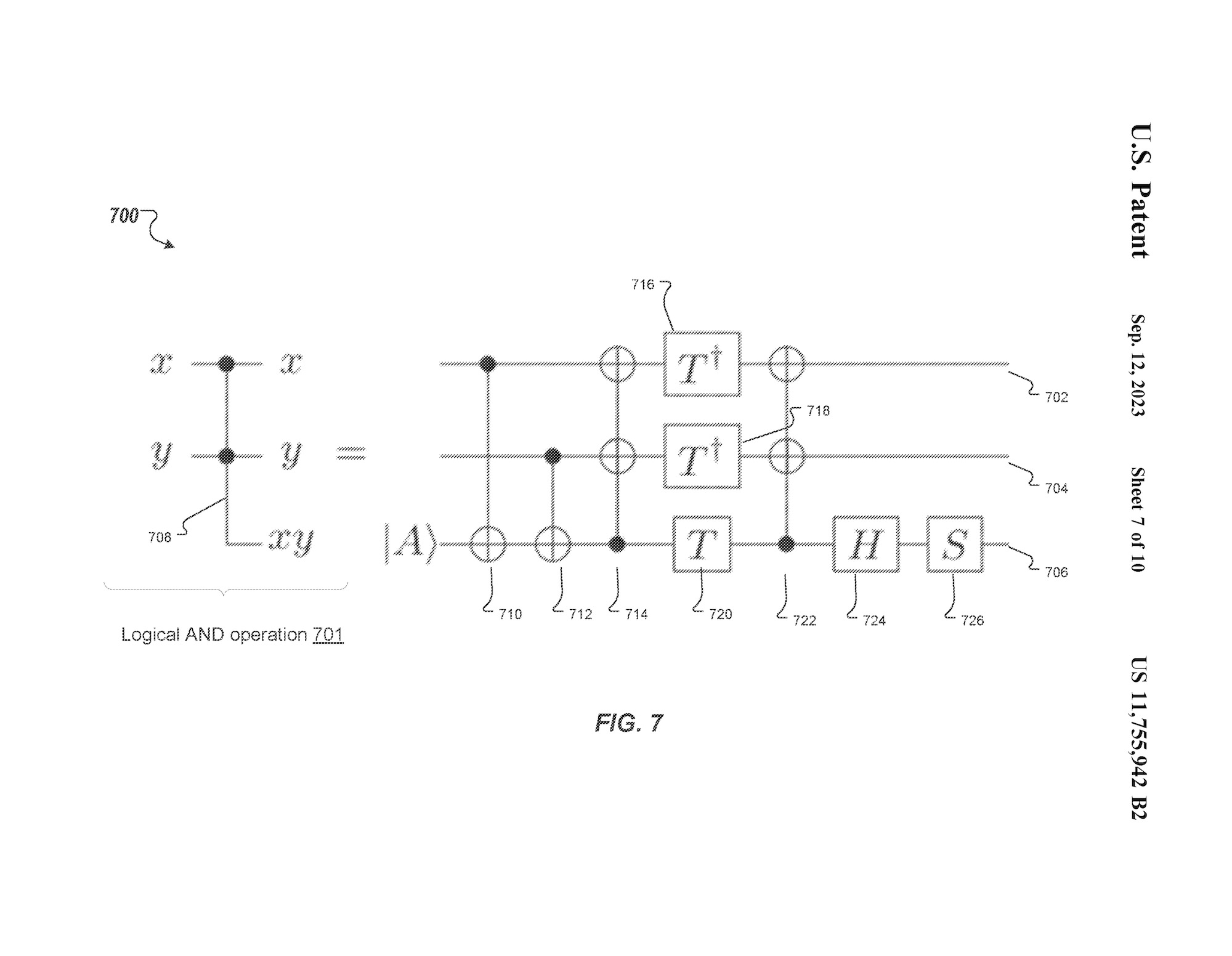
Figure Description: an exemplary quantum circuit for performing a temporary logical AND operation on two control qubits
Abstract: a method for performing a temporary logical AND operation on two control qubits includes the actions of obtaining an ancilla qubit in an A-state; computing a logical-AND of the two control qubits and storing the computed logical-AND in the state of the ancilla qubit, comprising replacing the A-state of the ancilla qubit with the logical-AND of the two control qubits; maintaining the ancilla qubit storing the logical-AND of the two controls until a first condition is satisfied; and erasing the ancilla qubit when the first condition is satisfied.
Training Quantum Evolutions using Sublogical Controls
9/19/2023 (US 11,763,187) [20 Claims, 3 Drawings]
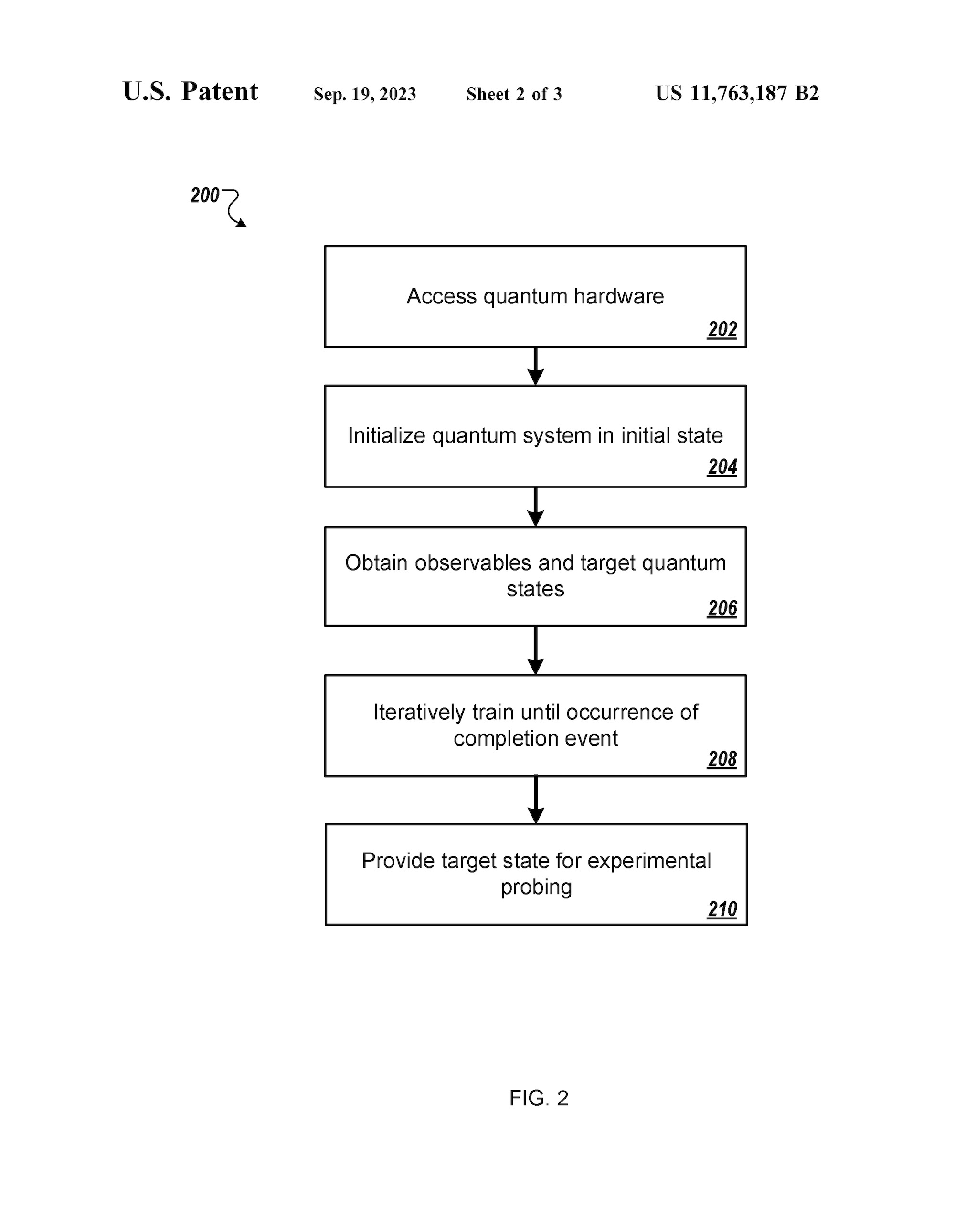
Figure Description: a flow diagram of an example process for training quantum evolutions using sublogical controls
Abstract: A method includes the actions of accessing quantum hardware, wherein the quantum hardware includes a quantum system comprising one or more multi-level quantum subsystems; one or more control devices that operate on the one or more multi-level quantum subsystems according to one or more respective control parameters that relate to a parameter of a physical environment in which the multi-level quantum subsystems are located; initializing the quantum system in an initial quantum state, wherein an initial set of control parameters form a parameterization that defines the initial quantum state; obtaining one or more quantum system observables and one or more target quantum states; and iteratively training until an occurrence of a completion event.
Refining Qubit Calibration Models Using Supervised Learning
(Publication) - 9/28/2023 (US 2023/0306292)
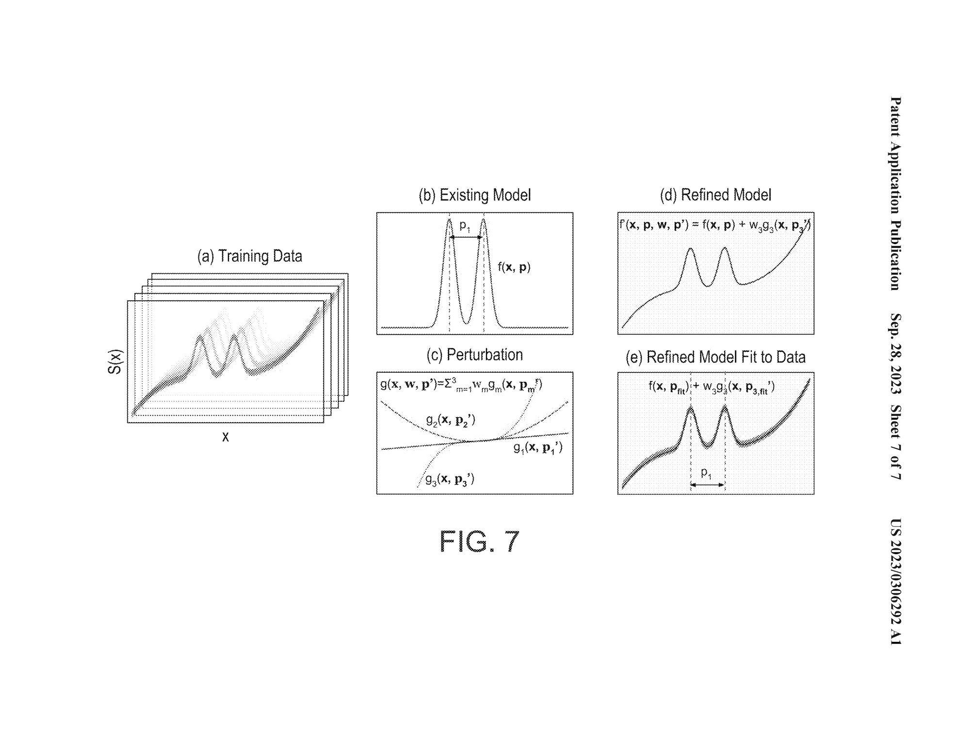
Figure Description: FIG. 7(a) is an illustration depicting calibration data; FIG. 7(b) is an illustration depicting an existing calibration model function; FIG. 7(c) is an illustration depicting a perturbation formed by three basis expansion functions; FIG. ( d ) is an illustration depicting a refined model; FIG. 7(e) is an illustration depicting a fit of the refined model to a calibration data set.
Abstract: Receiving, at a learning module, training data, wherein the training data comprises a plurality of calibration data sets, wherein each calibration data set is derived from a system comprising one or more qubits, and a plurality of parameter sets, each parameter set comprising extracted parameters obtained using a corresponding calibration data set, wherein extracting the parameters includes fitting a qubit calibration model to the corresponding calibration data set using a fitter algorithm. The method further comprises executing, at the learning module, a supervised machine learning algorithm which processes the training data to learn a perturbation to the qubit calibration model that captures one or more features in the plurality of calibration data sets that are not captured by the qubit calibration model, thereby to provide a refined qubit calibration model.
Microsoft
Evaluating Quantum Computing Circuits in View of the Resource Costs of a Quantum Algorithm
9/12/2023 (US 11,755,682) [20 Claims, 12 Drawing Sheets]
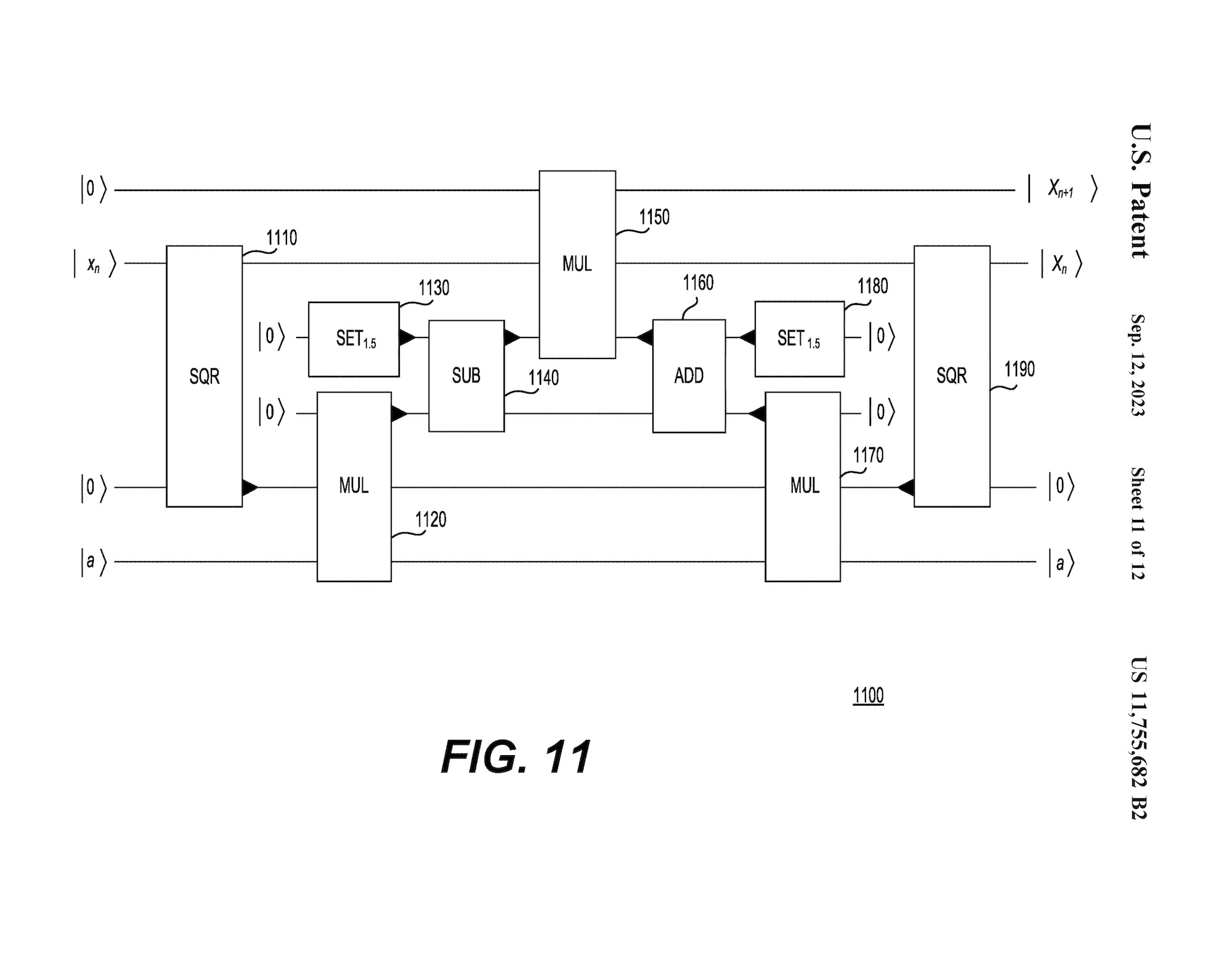
Figure Description: shows a circuit for the n-th Newton iteration of computing of the inverse square root of a variable in accordance with one example
Abstract: A processor-implemented method for performing an evaluation of a polynomial corresponding to an input is provided. The method includes determining a polynomial interpolation for a set of sub-intervals corresponding to the input. The method further includes constructing a quantum circuit for performing, in parallel, polynomial evaluation corresponding to each of the set of sub-intervals.
Geometry-Based Compression for Quantum Computing Devices
9/12/2023 (US 11,755,941) [20 Claims, 31 Drawing Sheets]
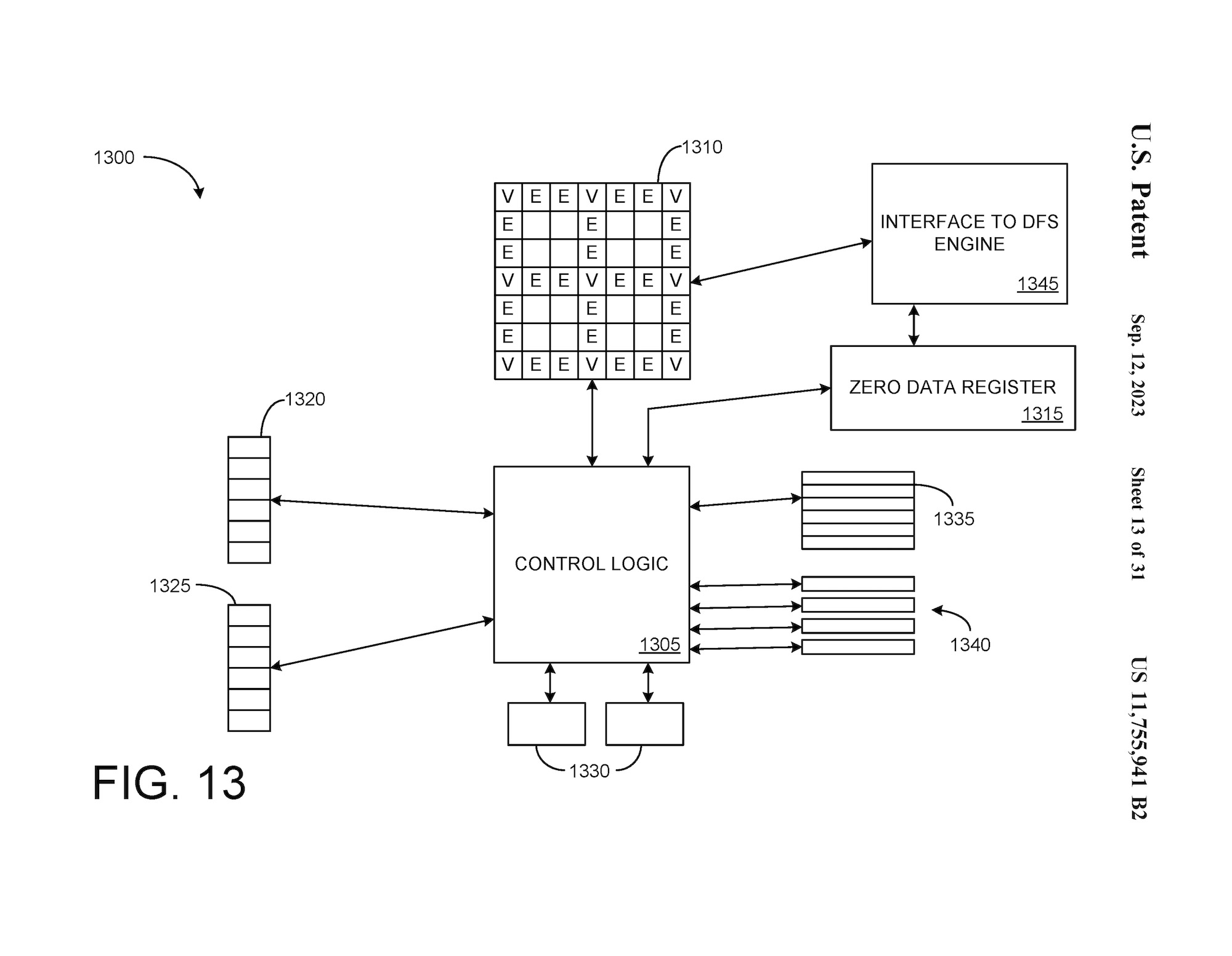
Figure Description: schematically shows an example Graph Generator module
Abstract: A quantum computing device comprises a surface code lattice that includes 1 logical qubits, where I is a positive integer. The surface code lattice is partitioned into two or more regions based on lattice geometry. A compression engine is coupled to each logical qubit of the 1 logical qubits. Each compression engine is configured to compress syndrome data generated by the surface code lattice using a geometry-based compression scheme. A decompression engine is coupled to each compression engine. Each decompression engine is configured to receive compressed syndrome data, decompress the received compressed syndrome data, and route the decompressed syndrome data to a decoder block.
Superconducting Quantum Interference Devices and Uses Thereof
(Publication) - 8/24/2023 (US 2023/0270019)
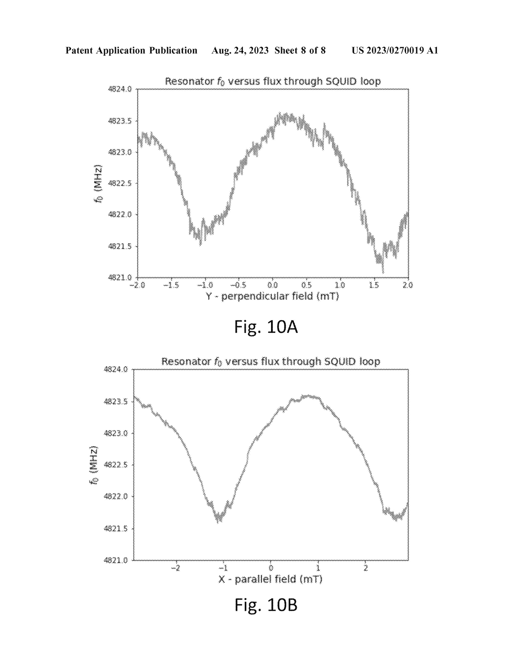
Figure Description: FIG. 10A is a plot showing the frequency response of the LC resonator circuit investigated in the Example to a magnetic field applied perpendicular to the plane of the substrate; and FIG. 10B is a plot showing the frequency response of the LC resonator circuit investigated in the Example to a magnetic field applied parallel to the plane of the substrate.
Abstract: A system comprises a substrate having a planar surface; a first magnet configured to apply a first magnetic field parallel to the planar surface; a circuit arranged on the planar surface; and a superconducting quantum interference device, SQUID, operably linked to the circuit. The SQUID comprises a Josephson junction arranged in a superconductive loop. The superconductive loop includes a portion which extends perpendicular to the planar surface and is orientated such that the SQUID is tuneable by the first magnet. By allowing the SQUID to be tuned using a magnetic field which is parallel to the planar surface, a reduction in flux noise may be achieved. Also provided are a method of operating a SQUID, and a SQUID.
JPMorgan Chase
Systems and Methods for Pixel-Based Quantum State Visualization
7/4/2023 (US 11,694,375) [16 Claims, 13 Drawing Sheets]
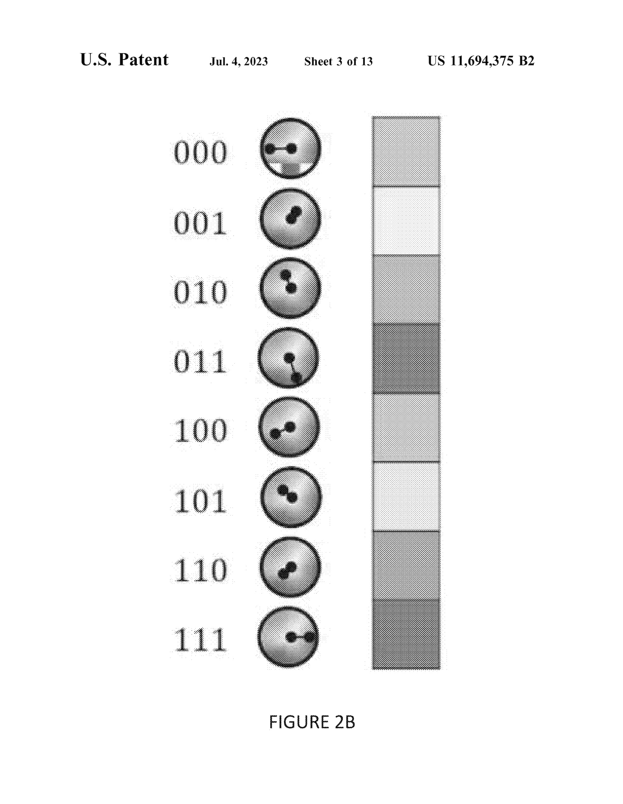
Figure Description: exemplary visualization of a 3-qubit state mapped to a hue according to an embodiment
Abstract: A computer-based method for generating a visualization of a quantum state may include: (1) receiving, at a computer program executed by a computer processor, quantum input data comprising a plurality of outcomes for a quantum state, each outcome having a phase and a magnitude; (2) for each outcome, translating, by the computer program, the outcome into a pixel having a hue based on the phase and an intensity based on the magnitude; (3) plotting, by the computer program, the pixel on a pixel graph; and (4) outputting, by the computer.
Systems and Methods for Zero-Footprint and Safe Execution of Quantum Computing Programs
11/22/2022 (US 11,507,397) [16 Claims, 2 Drawings]
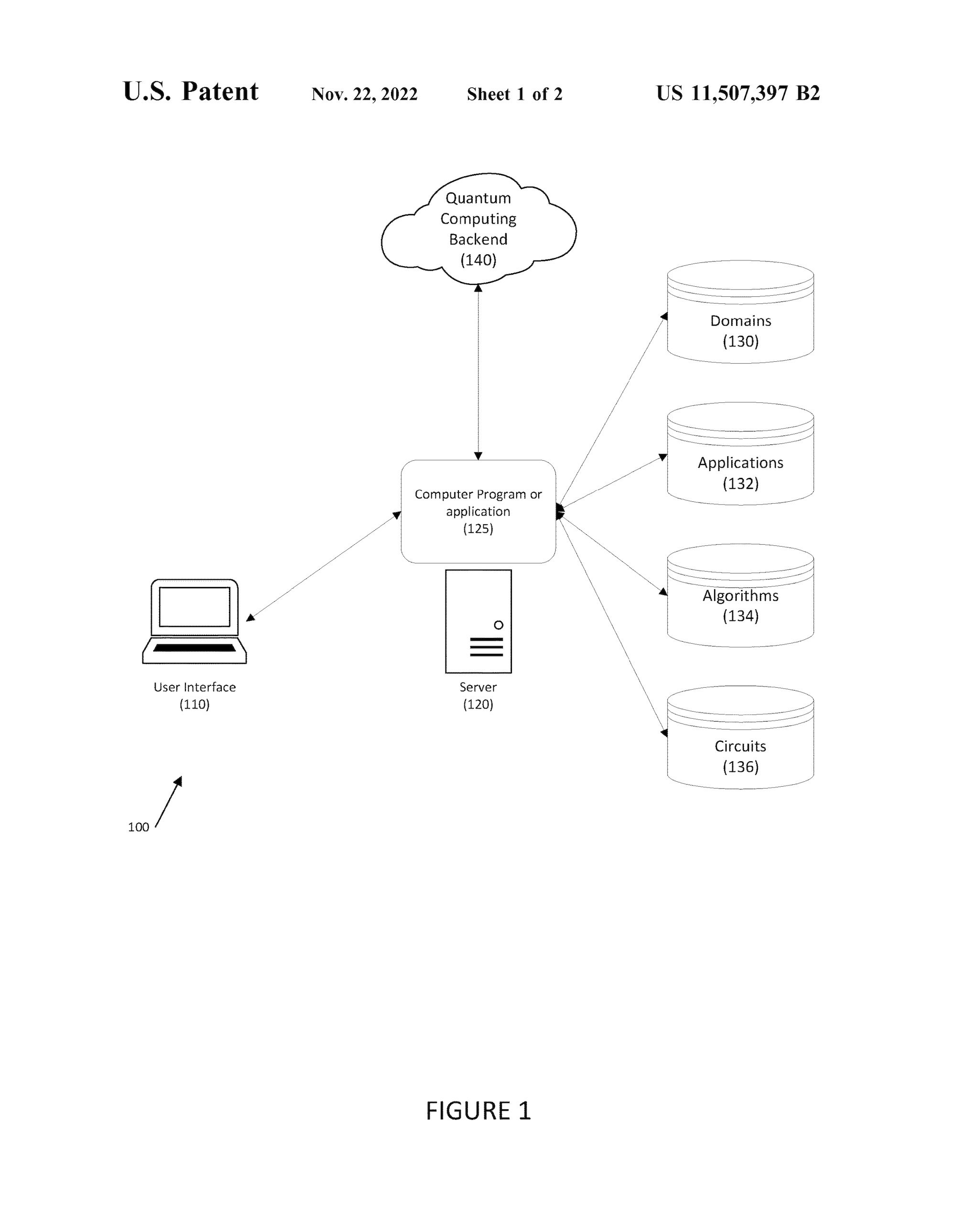
Figure Description: depicts a system for cloud-based execution of quantum-computing programs according to one embodiment
Abstract: An electronic device comprising at least one computer processor, a method for cloud-based execution of quantum-computing programs may include: (1) receiving, from a user interface on a client device, a serialized file comprising a domain, an application, and an algorithm; (2) receiving, from the user interface, problem data and an identification of a quantum computing backend for executing the problem data; (3) instantiating a quantum program for execution and communicating the quantum program and the problem data to the quantum computing backend for execution; (4) receiving, from the quantum computing back- end, an output of the execution; and (5) communicating the output to the user interface on the client device.
Wells Fargo Bank
Systems and Methods for Time-Bin Quantum Session Authentication
9/26/2023 (US 11,770,244) [20 Claims, 14 Drawings]
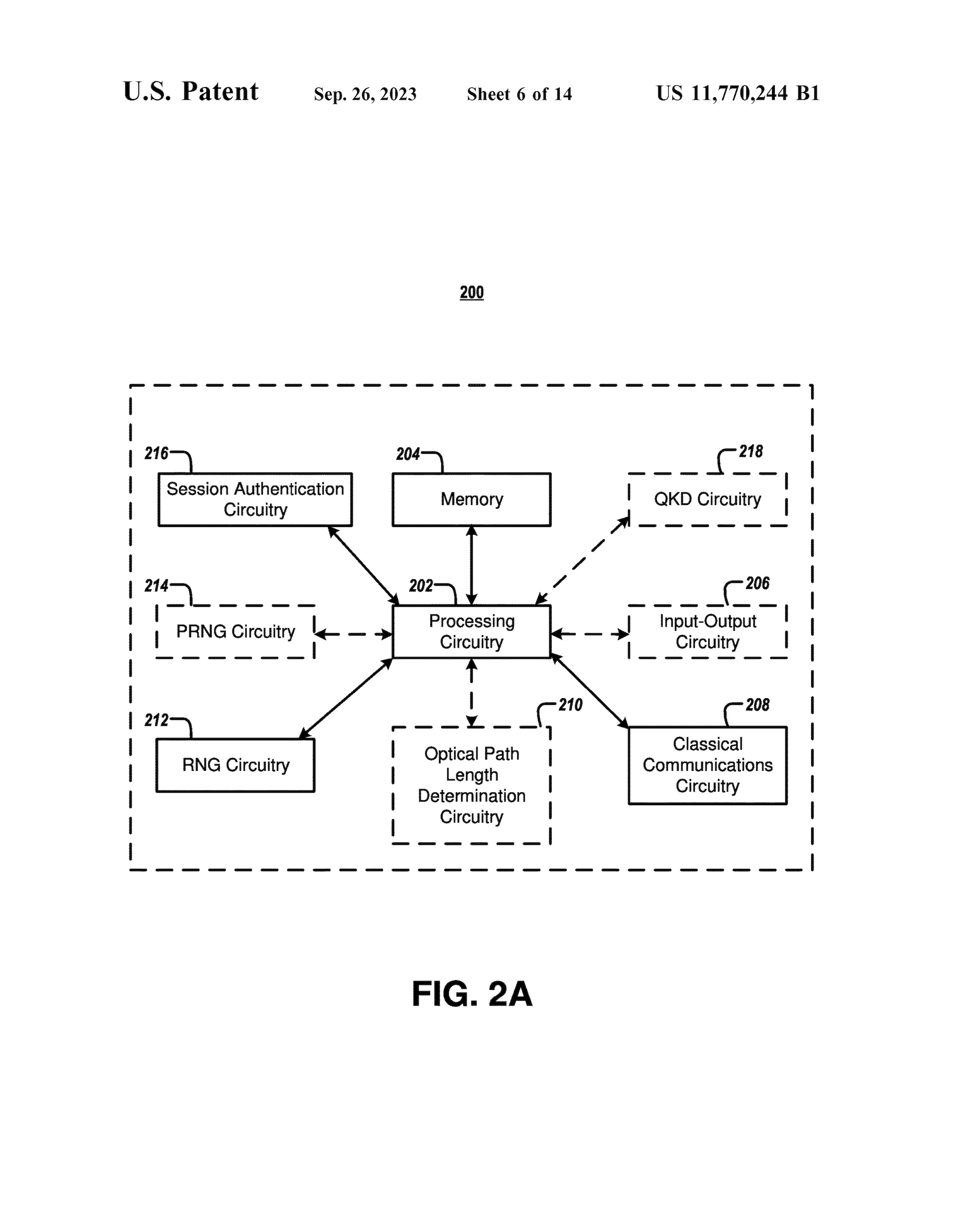
Figure Description: schematic block diagram of example circuitry
Abstract: Determining, by decoding circuitry, a set of optical path lengths to use for measurement. The example method further includes receiving, by the decoding circuitry, a set of time-bin qubits. The example method further measuring, by the decoding circuitry and based on the determined set of optical path lengths, the set of time-bin qubits to generate a set of bits.
Bank of America
Quantum Dynamic Network Sever Load Management System
(Publication) - 9/28/2023 (US 2023/0306296)
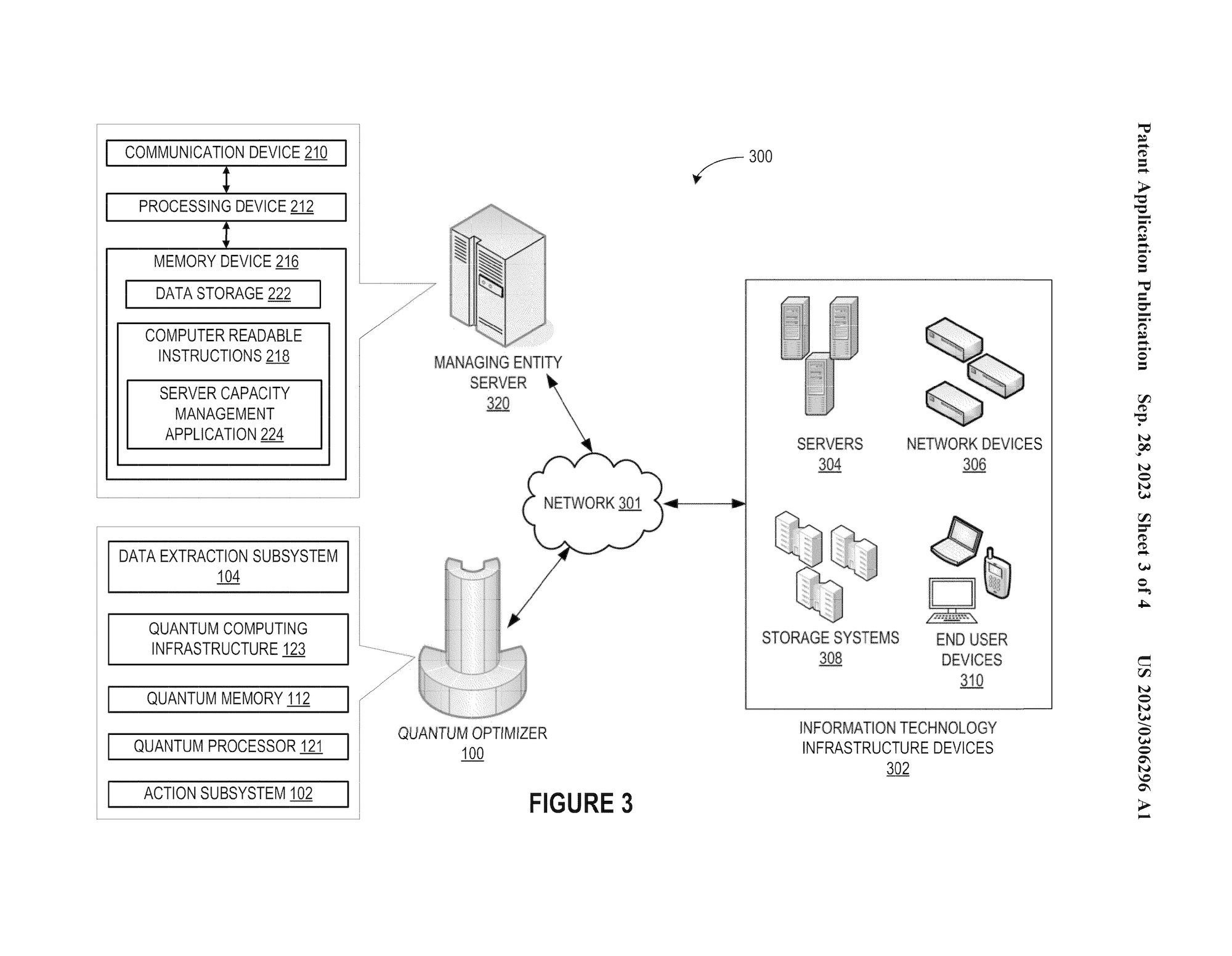
Figure Description: provides a block diagram illustrating a system environment for providing a quantum dynamic server load management system, in accordance with embodiments of the invention
Abstract: A system for using quantum optimization to provide a real time network server load or capacity management system for dynamic update and resource allocation and outage prevention. Load management information is received from a plurality of information technology infrastructure devices (e.g., servers, network devices, storage systems, and end user devices) that make up an overall system network environment. When at least a portion of that load management information is too burdensome for a conventional computer apparatus, the information is formatted for quantum optimization and transmitted to a quantum optimizer. The quantum optimizer analyzes the data and responds with an optimized load leveling or load balancing process for distributing traffic across the information technology infrastructure devices. This optimized load leveling process is then implemented across the appropriate devices.
Overview | Post-Quantum Cryptography | Patent Search | Trademarks | Copyrights | Videos